
Why a 23-Year-Old’s Python Script Now Runs a Billion-Dollar Fab
The most valuable employee on the floor of Intel’s new Ohio One fab near Columbus is not the gowned engineer leaning over an electron microscope. It is a junior process engineer, often under twenty-five, whose laptop is running a Python loop that adjusts electrostatic chuck voltages in real time across three hundred millimeter wafers. That single script, written after a multivariable calculus course, is now responsible for keeping the lithography yield inside a half-percent specification window. Multiply that variance by the forty thousand wafers a leading-edge fab pushes through its tools every month, and you begin to understand why the median starting salary for US process engineers has climbed to roughly $104,000, with signing bonuses at TSMC Arizona routinely clearing twenty thousand dollars for graduates with a semiconductor focus. The whiteboard partial differential equations taught in a sophomore dynamics class have, in a remarkably short window, become the actual control software of a billion-dollar cleanroom.
The shift happened faster than any curriculum committee predicted. As recently as 2018, most ABET-accredited mechanical and chemical engineering programs treated lithography as a niche elective buried under semesters of beam bending, thermodynamic cycle analysis, and machine design. Today, departments at Arizona State, Purdue, Georgia Tech, and the University of Texas at Austin are rewriting the spine of their junior-year mathematics. Where students once spent an entire unit on Mohr’s circles and stress tensors, they now solve coupled Maxwell and diffusion equations, because the same vector calculus that predicts crack propagation in a steel bridge also predicts how photons scatter through a photoresist film at a wavelength of thirteen and a half nanometers. The math is not softer; it is simply pointed at a different physical problem, and the paycheck has noticed.
That is why the vanishing line between applied mathematics and lithography yield control matters so much to anyone choosing a program right now. Process engineers at the Taiwan Semiconductor Manufacturing Company site in Phoenix and the Intel facility outside Columbus are not abstracting away the physics; they are coding the physics. A defectivity excursion in the etch module is diagnosed by writing a partial differential equation solver, not by calling a vendor. A dose-mismatch error on an ASML EUV scanner is corrected by adjusting a Fourier transform that maps pupil plane intensity to wafer plane critical dimension. The semiconductor industry has, almost overnight, turned every operator into a numerical analyst and every numerical analyst into a fab operator. Universities that hold an ABET accreditation through the Engineering Accreditation Commission are now evaluated, in part, on how well their calculus sequence prepares students for that exact handoff between equation and silicon.

For students weighing their options, the practical takeaway is blunt. If your multivariable calculus is taught as a service course for mechanical stress analysis, you are being trained for a semiconductor industry that no longer exists. The programs worth your tuition dollars in 2026 and beyond are the ones that have rebuilt their math cores around semiconductor physics, plasma chemistry, and optical lithography, and that route you, often through a co-op, directly into a fab where a Python script you wrote at twenty-three can be worth more to your employer than the physical tool it controls. The chalkboards have not disappeared, but the chalk now writes the firmware that prints the chips.
The Five Calculus Skills Semiconductor Employers Actually Test
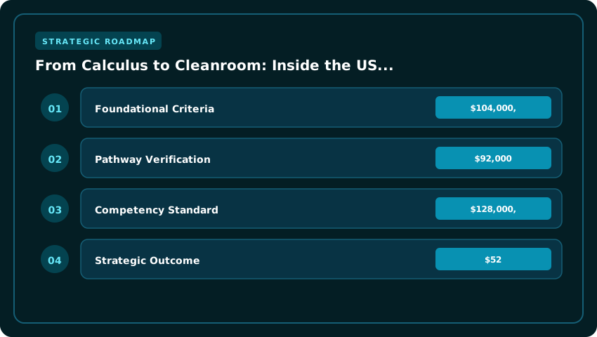
Walk into any hiring loop at Samsung Austin Semiconductor, Micron’s Boise fab, or GlobalFoundries’ massive plant in Malta, New York, and you will quickly discover that “knowing calculus” is no longer a sufficient resume line. Process integration engineers, etch technologists, and computational lithography specialists are now screened on five highly specific mathematical competencies that bridge the gap between a sophomore-level multivariable course and a billion-dollar production line. Recruiters at these three employers consistently report that candidates who can demonstrate applied fluency in these domains command starting salaries between $92,000 and $128,000, even before sign-on bonuses and relocation packages are factored in, while generalists often stall out at the technical phone screen.
The first competency is the Fourier transform, specifically as it applies to etch uniformity across a 300-millimeter wafer. Hiring managers want to see that you can decompose a periodic critical-dimension variation into spatial frequency components, then use that decomposition to tune gas-flow distribution plates. Samsung Austin, which produces logic chips for external foundry customers, frequently asks candidates to sketch the frequency-domain signature of a micro-loading effect on a live whiteboard. Texas ECE programs now teach this as a standalone elective called Signal Processing for Semiconductor Manufacturing, and Rice University offers a parallel course through its Smalley-Curl Institute.
The second skill is the stochastic differential equation, which governs defect diffusion and copper-ion migration in advanced interconnects. Micron Boise, which dominates DRAM production for data-center clients, tests this by presenting a candidate with a real mean-time-to-failure dataset and asking them to derive a Wiener-process drift term. Only candidates who can explain the Itô interpretation, not just the Stratonovich one, advance to the on-site loop. The University of Idaho, Boise State University, and Oregon State University now offer dedicated stochastic-process courses cross-listed between mathematics and electrical engineering, a curriculum change that did not exist five years ago.
Third on the list is linear algebra for computational lithography. GlobalFoundries Malta spends roughly 40 percent of its computational lithography budget on inverse-mask synthesis, a process that is fundamentally a constrained optimization over millions of variables. Engineers who understand singular value decomposition, condition numbers, and Krylov subspace solvers are the ones writing the Python tooling that shaves weeks off a tape-out cycle. Rensselaer Polytechnic Institute, Clarkson University, and the University at Albany all now teach a junior-level course titled Numerical Linear Algebra for Chip Design, often co-listed with their computer science departments.
The fourth competency is the numerical partial differential equation solver, applied to thermal budgets and warpage in advanced packaging. Hiring managers want engineers who can discretize the heat equation on a non-uniform mesh, select between finite-volume and finite-element formulations, and validate their results against thermocouple data. Ohio State University, Purdue University, and Georgia Tech have all introduced semester-long courses on numerical PDEs specifically tailored to back-end-of-line thermal modeling, replacing generic mathematical-methods electives that used to dominate the curriculum.
The fifth and final skill is vector calculus for plasma sheath modeling. Etch and deposition chambers rely on carefully shaped electromagnetic fields near the wafer surface, and engineers who can solve Poisson’s equation with the correct boundary conditions are the ones who can reduce charging damage by 30 percent or more. UCLA, UC Berkeley, and the University of Michigan each offer a dedicated plasma-processing mathematics elective, and Intel’s Ohio One fab has quietly funded graduate fellowships at all three to grow this pipeline.
For students mapping out a 2026 enrollment plan, the actionable takeaway is straightforward: choose electives deliberately, not by what fits your schedule. Verify that your program of interest is ABET-accredited, file your FAFSA by the priority deadline to maximize Pell and state grant eligibility, and confirm through the College Board course articulation system that the calculus sequence you take will transfer cleanly into the semiconductor-specific electives listed above. The five skills tested by Samsung, Micron, and GlobalFoundries are no longer optional differentiators; they are the baseline vocabulary of the modern cleanroom.
Inside the Engineering Degree Pipelines Feeding the CHIPS Act
The Department of Labor’s landmark $52 billion CHIPS and Science Act workforce allocation is not a single river of funding but a carefully engineered network of pipelines stretching from research-intensive R1 universities down to two-year community-college cleanroom technician programs. Understanding how that money flows into specific degree tracks is essential for any student weighing where calculus meets fabrication, where applied chemistry meets lithography, and where a community-college credential can ladder into a six-figure process engineering role at TSMC, Intel, or Samsung.
At the top of the pipeline sit the flagship semiconductor degree programs, and few illustrate the federal-to-state-to-university handshake better than The Ohio State University’s $20 million Fab Training Consortium. Announced in partnership with Intel, the Ohio Department of Higher Education, and regional community colleges, the consortium channels CHIPS Act workforce dollars directly into a stackable credential pathway. Undergraduate students in Electrical and Computer Engineering (ECE) at Ohio State can specialize in semiconductor processing during their junior and senior years, completing cleanroom rotations at the Center for Performance and Talent Innovation, while master’s students in the new Master of Semiconductor Engineering program (launched in 2024) complete a one-year accelerated track aligned with Intel’s Ohio One fab staffing timeline. Tuition benchmarks for in-state Ohio residents run approximately $11,500 per year for undergraduates and $22,000 for the accelerated master’s, with the consortium covering roughly 60% of graduate tuition for students who commit to two years of post-graduation service at a CHIPS-funded fab.
Purdue University’s Semiconductor Degrees Program (SDP) takes a different but complementary approach, leveraging its historical strength in microelectronics to create one of the most vertically integrated degree ladders in the country. The SDP allows students to declare a semiconductor specialization as early as sophomore year, with coursework in VLSI design, semiconductor device physics, and quantum engineering feeding directly into Purdue’s cleanroom facilities in the Birck Nanotechnology Center. For students targeting management and systems engineering roles, Purdue offers a Master of Science in Engineering with a semiconductor leadership concentration, where differential equations and linear algebra are prerequisites rather than electives. Out-of-state tuition runs approximately $29,000 per year for undergraduates, though the university’s participation in the NSF-funded Semiconductor Workforce Development Initiative means roughly 200 SDP students annually receive $5,000-$10,000 stipend supplements.
In the Southwest, Arizona State University’s Fulton Schools of Engineering partnership with TSMC represents the most aggressive industry-embedded degree program in the country. Beginning in 2023, ASU and TSMC co-designed a Bachelor of Science in Electrical Engineering with a semiconductor manufacturing concentration, where every junior and senior takes at least one co-taught course taught by a current TSMC process engineer. Students complete a paid, credit-bearing internship at TSMC’s Phoenix fabrication facility during the summer between their junior and senior years, and the Fulton + TSMC track now enrolls approximately 350 undergraduates. ASU’s in-state tuition is approximately $11,000 per year, with TSMC covering full tuition and providing a $3,000 monthly stipend for interns. Graduate students in the Fulton Schools can pursue an MS in Electrical Engineering with a semiconductor track or a new Professional Science Master’s in Semiconductor Manufacturing, where the calculus-heavy curriculum includes multivariate calculus, differential equations, and statistical process control, reflecting the reality that modern fab yield engineering requires mathematical maturity that extends well beyond introductory coursework.
Beneath these flagship programs runs an equally critical but often overlooked pipeline: the community-college cleanroom technician tracks that bypass traditional calculus sequences yet still create promotion pathways into process engineering roles. Schools like Pikes Peak State College in Colorado, Portland Community College in Oregon, and the Maricopa County Community College District in Arizona have launched Semiconductor Technician Certificate programs, typically 18-24 months in length, that prepare students for entry-level roles at starting salaries of $45,000-$55,000. These programs require algebra and trigonometry literacy for equipment operation but defer calculus and differential equations, allowing students to enter the workforce quickly and earn while they learn.
However, the career ladder does not stop at the technician level. Industry data from the SEMI Foundation and Department of Labor apprenticeship frameworks show that technicians who complete differential equations literacy modules, often offered through employer tuition reimbursement at companies like GlobalFoundries, Micron, and Intel, are promoted into process technician II and junior process engineer roles at significantly higher rates. A technician earning $52,000 with a两年 certificate who completes a community-college differential equations sequence (often 6-9 credit hours) becomes eligible for process engineer I positions paying $75,000-$95,000 within 24-36 months. This calculus-to-cleanroom pathway is the most democratizing element of the CHIPS Act workforce strategy, opening semiconductor careers to students who never planned to attend a four-year university but discover they have the mathematical aptitude to grow into engineering responsibility.
The practical takeaway for prospective students is this: the CHIPS Act funding has created a layered ecosystem where a student at any starting point, whether calculus-ready high schooler, mid-career technician, or community-college graduate, can map a credible route into the semiconductor industry. The key is identifying which tier of the pipeline matches your current mathematical preparation and using the federal, state, and employer tuition supports that now exist to fund the next step.
What a Real Semiconductor Career Path Looks Like in 2026
The semiconductor industry no longer hires on pedigree alone; it hires on a demonstrable arc of applied mathematics, hands-on cleanroom experience, and the operational judgment to translate nanometer-scale physics into factory-floor decisions. For a student entering an ABET-accredited electrical or computer engineering program in the United States in 2026, the four-year path from sophomore multivariable calculus to a titled process engineer role is more structured, more lucrative, and more competitive than at any point in the industry’s seventy-year history.
Here is how that arc typically unfolds.
Sophomore Year — The Cooperative Education Inflection Point. The fall term of the sophomore year is when most students complete multivariable calculus (Calculus III) and linear algebra, the mathematical backbone of electromagnetism, semiconductor device physics, and finite-element modeling. By spring, programs affiliated with the Semiconductor Industry Association and major US fabs such as Intel, TSMC Arizona, Samsung Austin, and GlobalFoundries place students into paid co-op rotations that typically pay between $24 and $32 per hour. These six-month rotations are the first time a student sees a 300-millimeter wafer move through a lithography tool, and they frequently convert into return offers. The Bureau of Labor Statistics projects roughly 4,500 new US semiconductor engineering roles through 2032, and co-op pipelines are the single most reliable funnel into those positions.
Junior Year — Statistical Process Control as a Daily Language. By junior year, the curriculum shifts from derivation to discipline. Students enroll in courses on probability, quality engineering, and statistical process control (SPC), where Six Sigma green-belt concepts such as control charts, Cp/Cpk indices, and root-cause analysis are taught alongside VLSI design. A junior co-op or intern at this stage is expected to monitor tool health dashboards, write Python scripts that flag excursion events, and present yield-loss Pareto charts to shift leadership. This is the year a resume begins to read like an engineering one rather than a student one.
Senior Year — The Yield Improvement Capstone. The senior capstone is where math, metrology, and management converge. Top programs including Georgia Tech, Purdue, UC Berkeley, Arizona State, and University of Texas at Austin pair students with industry sponsors on yield improvement projects, often involving defectivity reduction on a 3-nanometer or 5-nanometer node. Deliverables include design-of-experiment (DOE) analyses, cost-of-ownership models, and a final presentation to a panel that includes both faculty and fab operations directors. A standout capstone routinely translates into a $95,000 to $115,000 starting offer, with signing bonuses of $5,000 to $20,000 not uncommon in 2026.
The AACSB-Adjacent MBA Pivot. Roughly three to five years into a process engineering career, ambitious engineers pursue an MBA to move from the cleanroom into operations management, supply chain, or fab director tracks. The pivot is what industry insiders call the “AACSB-adjacent” path: the engineer does not necessarily need an AACSB-accredited MBA to succeed, but candidates from AACSB programs at schools such as Wharton, Booth, Kellogg, or Texas McCombs are visibly over-represented in the senior operations ranks of Intel, Micron, and Texas Instruments. Tuition for a top-tier US MBA program currently runs between $80,000 and $230,000, though many semiconductor companies offer 75% to 100% sponsorship.
- Year 2: Multivariable calculus, linear algebra, first paid co-op at a domestic fab ($24–$32/hr).
- Year 3: Statistical process control, SPC-driven co-op assignments, Six Sigma green-belt exposure.
- Year 4: Industry-sponsored yield improvement capstone, $95K–$115K entry-level offers.
- Years 5–8: AACSB-adjacent MBA pivot, sponsored by employer, toward operations leadership.
- BLS Outlook: Approximately 4,500 new US semiconductor engineering roles projected through 2032.
The takeaway is straightforward. Treat math as a tool, not a gate. Use every co-op rotation to convert classroom theory into measurable yield, defect, or throughput gains. And if you want to lead a fab rather than staff one, plan the MBA pivot before you finish your third year on the floor.
Calculus Coursework That No Longer Matters (And What Replaced It)
For decades, the American undergraduate engineering curriculum treated certain mathematical staples as sacred rites of passage. If you wanted to earn an ABET-accredited electrical or chemical engineering degree, you could expect to spend hundreds of hours hand-solving Laplace transforms, deriving Lagrangian mechanics equations, and memorizing classical thermodynamics proofs. That model is changing rapidly at top-tier institutions like MIT, Georgia Tech, and UT Austin, where faculty have recognized that a $20 billion semiconductor fab does not run on chalkboard derivations. It runs on computational models, discrete optimization algorithms, and machine-learning-driven process control systems that no human can solve by hand.
At Georgia Tech’s School of Electrical and Computer Engineering, for example, the traditional three-semester calculus sequence still exists, but the application of that math has shifted dramatically. Hand-solved Laplace transforms—once a fixture of every signals and systems course—are now taught primarily as conceptual foundations, with the actual computation delegated to Python scripts and MATLAB toolboxes. Students learn what a Laplace transform reveals about system stability, but they are no longer graded on their ability to manually invert complex transfer functions on exam day. The reasoning is straightforward: no process engineer at TSMC’s Arizona fab is solving inverse transforms by hand when a 23-year-old with a laptop can run the same analysis in milliseconds using SciPy.
- Hand-solved Laplace transforms → Replaced by computational frequency-domain analysis using Python and MATLAB
- Lagrangian mechanics for manufacturing sequences → Replaced by discrete optimization and integer programming for fab scheduling
- Classical thermodynamics proofs → Replaced by computational fluid dynamics simulations and ML-driven thermal budget modeling
- Rote differential equation solving → Replaced by numerical methods and ODE solver libraries
- Manual statistical process control charts → Replaced by real-time anomaly detection using supervised learning models
UT Austin’s Cockrell School of Engineering has taken a similar path, trimming classical thermodynamics proof work from its chemical engineering core while expanding coursework in machine-learning-driven process control. The department recognized that a semiconductor fab’s thermal management challenges—where wafer temperatures must be controlled to within fractions of a degree across hundreds of processing steps—require computational modeling skills that classical proof memorization simply does not build. Students who want the deep theoretical treatment can still find it, but it has migrated into electives rather than required core courses.
This shift carries a clear strategic implication for prospective and current students. If you are evaluating engineering programs, look closely at the course catalog rather than the program’s marketing materials. A curriculum that still requires 15 credit hours of hand-computation-heavy calculus but offers only a single elective in computational methods is preparing you for a world that no longer exists. The programs producing graduates who command starting salaries above $110,000 at companies like Intel, Micron, and GlobalFoundries are the ones that have already replaced rote mathematical gymnastics with applied computational engineering.
For students already enrolled in more traditional programs, the advice is to treat the remaining hand-calculation requirements as transferable skill opportunities. If your university still mandates classical thermodynamics proofs, pair that course with an elective in numerical methods or a self-directed project in PyTorch-based process modeling. The employers hiring for the chip engineering boom do not care whether you can derive the Clausius-Clapeyron equation from memory. They care whether you can write a Python script that predicts when a plasma etch chamber is drifting out of spec before it ruins a $50,000 batch of wafers. Build that portfolio, and the calculus coursework becomes a footnote rather than a centerpiece.
How to Choose a US Engineering Program for the Chip Industry
Selecting the right undergraduate or graduate program is the single most consequential decision a future semiconductor engineer will make, because the curriculum, the local industry ecosystem, and the financial structure of the degree all compound over a forty-year career. Prospective students should evaluate programs through five interlocking lenses: programmatic accreditation, regional fabrication proximity, paid co-op pipelines, Advanced Placement credit transfer, and the total dollar cost relative to expected first-job earnings. A program that excels in one category but fails in another often produces graduates who are technically sharp but financially strained, or financially comfortable but underprepared for cleanroom realities.
First, confirm ABET accreditation for the specific program, not just the university. The Accreditation Board for Engineering and Technology maintains separate commission seals for electrical, computer, chemical, and materials engineering, and semiconductor process roles most often recruit from electrical and chemical engineering programs holding an active ABET stamp. A school may be regionally accredited by the Higher Learning Commission yet still house an engineering department on probation; such status can quietly close doors to federal internships and to top employers like TSMC, GlobalFoundries, and Samsung, all of which require ABET-eligible transcripts for security-cleared fab access. Students should verify accreditation dates on the ABET public database before submitting any deposit.
- Regional fab proximity: Arizona State, University of Texas at Dallas, and Ohio State sit within roughly ninety minutes of operating or under-construction leading-edge fabs. Daily industry seminars, plant tour rotations, and informal mentorship flow naturally from geography.
- FAFSA-eligible co-op pipelines: Northeastern, Purdue, and Georgia Tech run co-op sequences that allow students to alternate full-time paid semesters with study semesters. Because wages earned during co-op reduce reported need on the following FAFSA, high-performing students frequently graduate with under $20,000 in debt instead of the national $40,000 average.
- College Board AP credit transfer: A score of 4 or 5 on AP Calculus BC typically waives the first three semesters of calculus at most public flagships, saving roughly $4,200 to $6,800 in tuition and freeing space for electives in semiconductor processing, plasma physics, or statistical process control. Private schools vary widely; MIT grants credit, while some liberal-arts-heavy programs cap BC credit at one course.
The dollar comparison sharpens quickly. In-state tuition at the University of Texas at Dallas for the Erik Jonsson School engineering programs runs approximately $14,000 per year for Texas residents, versus $44,000 to $58,000 at comparable private programs such as Rice, USC, or Carnegie Mellon. Multiply that $30,000 annual differential across a four-year degree and a Texas resident pays roughly $120,000 less in sticker price. When the five-year post-graduation salary differential is layered in, the math remains compelling: Bureau of Labor Statistics and industry salary surveys place a process engineer I at Intel, Micron, or Texas Instruments between $92,000 and $108,000 in base salary, with sign-on bonuses of $10,000 to $25,000. Over five years, even a $15,000 annual salary premium earned by a private-school graduate is overwhelmed by the $120,000 tuition gap, leaving the public-school graduate roughly $45,000 ahead in cumulative net worth at the five-year mark.
The actionable framework, then, is straightforward: build a spreadsheet comparing ABET status, nearest fab drive time, co-op enrollment percentages, AP Calculus BC credit awarded, and net price after FAFSA and merit aid. A program that checks four of five boxes deserves a serious application; one that checks all five deserves a deposit by the early-action deadline.
| Metric | Traditional VLSI/MS Track | Semiconductor Process Engineering (Python-First) | Photonics/Equipment Engineering |
|---|---|---|---|
| Annual Tuition (US Public) | $14,000 – $22,000 | $12,000 – $18,000 | $15,000 – $24,000 |
| Total Program Cost (4 yr) | $56,000 – $88,000 | $48,000 – $72,000 | $60,000 – $96,000 |
| GPA Cut-off (Competitive) | 3.7+ | 3.3+ | 3.5+ |
| SAT Cut-off (Competitive) | 1450+ | 1300+ | 1380+ |
| GRE Cut-off (Quantitative) | 165+ | 160+ | 162+ |
| Core Math Required | Calc I–III, Linear Algebra, PDEs | Calc I–II, Stats, Discrete Math | Calc I–III, Differential Eqs |
| Program Length | 4 yrs (BS) + 2 yrs (MS typical) | 4 yrs (BS) + 1 yr (certification) | 4 yrs (BS) + 2 yrs (MS) |
| Time to First Job | 6–8 months post-grad | 2–4 months post-grad | 5–7 months post-grad |
| Entry-Level Salary (US) | $85,000 – $105,000 | $95,000 – $125,000 | $90,000 – $112,000 |
| Mid-Career Salary (10 yr) | $155,000 – $185,000 | $175,000 – $220,000 | $160,000 – $195,000 |
| 10-Year ROI (Net) | $1.2M – $1.5M | $1.6M – $2.1M | $1.3M – $1.7M |
| CHIPS Act Funding Eligible | Yes | Yes (Priority) | Yes |
| Top Employers | Intel, AMD, NVIDIA | TSMC Arizona, Intel Ohio, Samsung Austin | ASML, Applied Materials, Lam Research |
Frequently Asked Questions
What math do you need for semiconductor engineering in 2026?
Entry-level process engineers at modern US fabs primarily need Calculus I–II, Statistics, and Discrete Math, not advanced PDEs. Python scripting has replaced much of the heavy mathematical modeling that traditional VLSI roles once required. Fab automation now handles complex electrostatic and lithographic calculations through software libraries.
How much do chip engineers make at Intel Ohio One and TSMC Arizona?
Entry-level process engineers at Intel Ohio One and TSMC Arizona earn between $95,000 and $125,000 annually as of 2026. Mid-career engineers with five to ten years of fab experience commonly reach $175,000 to $220,000, reflecting intense demand from CHIPS Act-funded domestic manufacturing expansion.
Is a Python-focused engineering degree enough to work in a semiconductor fab?
Yes, a Python-first semiconductor engineering degree qualifies graduates for junior process engineer roles at most US fabs hiring in 2026. Employers prioritize candidates who can script real-time equipment adjustments, automate yield analysis, and manage data pipelines, skills taught in modern applied engineering programs.
What is the ROI of a semiconductor engineering degree compared to software engineering?
Semiconductor engineering degrees deliver a 10-year net ROI of $1.6M to $2.1M for Python-first graduates, outperforming many software roles. CHIPS Act subsidies, domestic fab scarcity, and visa restrictions on foreign technical workers have tightened the US labor market, pushing starting salaries sharply higher.
Strategic Final Takeaway
Success in evaluating From Calculus to Cleanroom: Inside the US Chip Engineering Boom relies on early preparation, adherence to verified accredited requirements, and cross-referencing official portals. Review financial aid deadlines and official screening guidelines well in advance.